DESIGN, PACKAGING AND CHARACTERISATION OF PHOTONIC INTEGRATED CIRCUITS: THE SECOND MODULE OF PHOTONICS COURSES STARTS AT THE TECIP INSTITUTE
The first edition of the second module of "Photonic Integrated Circuits Design, Fabrication & Packaging" and “Photonic and Electronic Integrated Circuit Packaging” organized by the Photonics Integrated Technologies Center INPHOTEC of the Institute of Communication, Information and Perception Technologies (TeCIP) of Scuola Superiore Sant'Anna, in collaboration with the National Inter-University Consortium for Telecommunications (CNIT) will be held from 14 to 17 November.
This second meeting covers one module of 3-module course, for a total duration of 4 weeks program, which can also be attended individually, and is aimed at strengthening skills in the design, fabrication and packaging of photonic integrated circuits.
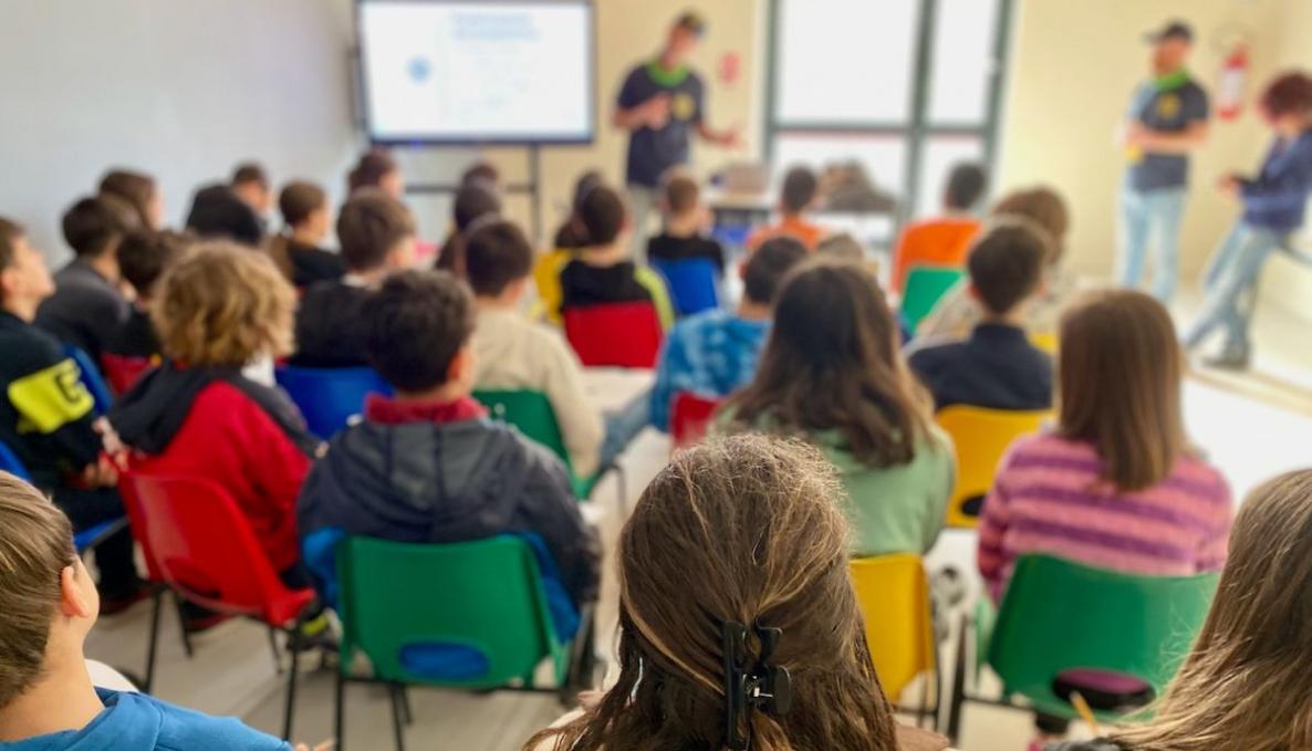
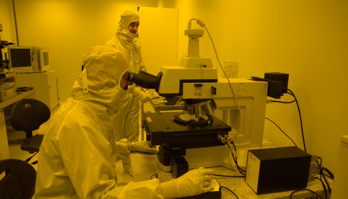
For the entire duration of the event the Photonic Integrated Circuits are the main players: participating in this event gives us all a great opportunity to focus on strategic issues and, through lectures and laboratory exercises, to interact with a unique infrastructure in Italy - the Clean Room - which operates in a highly strategic environment oriented towards design sessions within the front-end (fabrication) and back-end (packaging) infrastructures.
The Integrated Photonic Technologies Center of the Sant’Anna School of Advanced Studies of Pisa has been fully operational since 1st January 2015, created with a contribution provided by the Regione Toscana. 700 square meters are dedicated to clean rooms and it has four technological platforms: Silicon Photonics, Glass in Silicon, Hybrid Integration and Advanced Packaging.
Next events will be the Characterization and Testing (C & T) Session from 20 to 24 March 2017.
More on INPHOTEC and TeCIP Institute on this video.
For further details, please find attached the meeting brochure.