PHOTONICS: REGISTRATION NOW OPEN FOR cOURSES ON Integrated Circuit Design, Fabrication & Packaging
The aim of the courses promoted by the Integrated Photonic Technologies Center INPHOTEC of the Communication, Information and Perception Institute (TeCIP) of the Sant’Anna School of Advanced Studies, in collaboration with the National Inter-University Consortium for Telecommunications (CNIT), is to strengthen skills in the design, fabrication and packaging of photonic integrated circuits.
Registration for the first edition, free of charge, is open until the 2nd of May and is addressed to candidates both from the academic and industrial fields, with a degree in the area of Electronic or Telecommunication Engineering or Physics, or professionals with an adequate background willing to develop specific and comprehensive skills upon the complete line of design, fabrication, packaging and characterisation of photonic integrated circuits.
The entire cycle, for a total duration of four weeks, is divided into three modules, which can also be attended separately:
1. Photonic Integrated Circuit Design and Fabrication (PIC D&F) - 5-16 September 2016
2. Photonic and Electronic Integrated Circuit Packaging (PEIC Pack) - 14-18 November 2016
3. Characterization and Testing (C&T) session - 20-24 March 2017
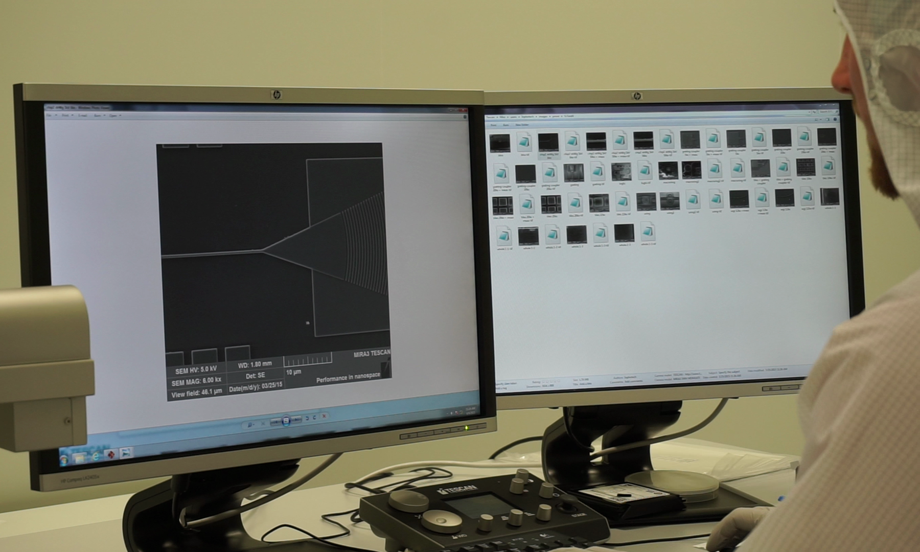
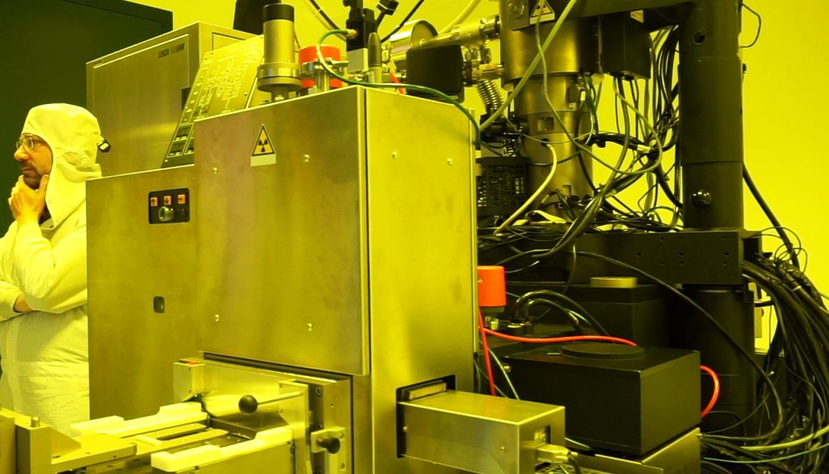
The first two modules include front lessons, laboratory exercises oriented towards design and “clean room” sessions within the front-end (fabrication) and back-end (packaging) infrastructures. During the third module, the participant will create the characterization and testing of the circuit that he/she has designed and which has been produced by the INPHOTEC staff.
Operational since the 1st of January 2015, the Integrated Photonic Technologies Center of the Sant’Anna School of Advanced Studies of Pisa was created with a contribution provided by the Regione Toscana. It counts 700 square meters of clean rooms and has four technological platforms: Silicon Photonics, Glass in Silicon, Hybrid Integration and Advanced Packaging.