Master’s Degree in Photonic Integrated Circuits designed by Sant’Anna School TECIP Institute: the European Commission has announced funding of over 3 million
The European Commission has selected the Institute TECIP (Communication, Information and Perception Technologies) of Sant’Anna School to receive a grant of over 3 million to finance the Erasmus Mundus Joint Master Degree, a two-year program aimed at training talented students in the design, creation and assessment of innovative integrated devices based on photonic technologies.
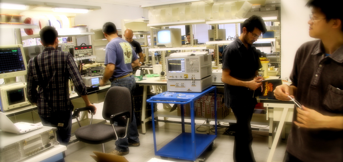
The team of researchers led by Professor Piero Castoldi at the INPHOTEC centre has been awarded the Erasmus Mundus Joint Master Degree project for the Photonic Integrated Circuits, Sensors and Networks (PIXNET) course, a master’s program jointly delivered by an international consortium of top level higher education institutions: the Technische University Eindhoven (The Netherlands), Aston University (UK) and Osaka University.
The program serves as an excellent training for the theoretical design of telecommunication system devices and the adoption of photonic integrated circuits to deal with the huge amounts of data that will be created by the Internet of Things.
PIXNET intends to be an interdisciplinary, multi-national initiative, training young telecommunication and electrical engineers. The adoption of Photonic Integrated Circuits (PIC) as a central element in the evolution of information networks will focus towards innovative packaging and integration schemes to deliver large volumes of data and compact switching devices in computing architectures. The PIXNET local path will take place at the Sant’Anna School in Pisa and its classes will be shared with the students following the international path.
The INPHOTEC centre (founded in 2015) at the TECIP Institute has been particularly successful in this call. Researchers at INPHOTEC work on optical networks and integrated photonics facilitating energy efficient data movement in future data communications systems. Their work is recognized internationally receiving support from Italian Government and international sources.
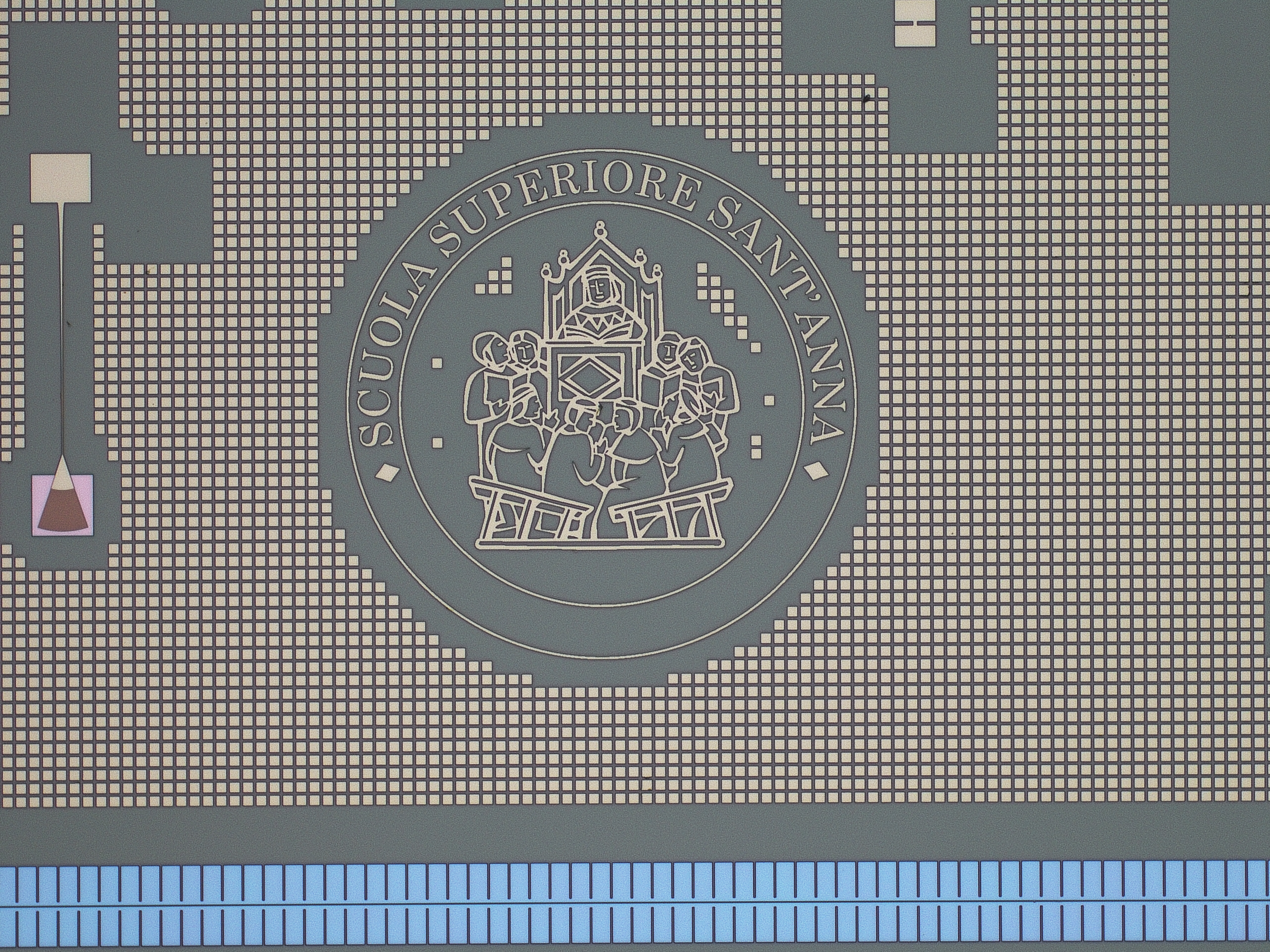
Multiple photonic integrated circuits offer the advantage of piece-wise manufacturing, packaging, and assembly, potentially reducing the number of optical I/O and electrical contacts on a single die. Integrating more photonic devices in micron-scale proximity on a computer chip will enable transistors, memory, modulators, and detectors to work together. Integration will lead to information moving faster and more efficiently, while using less power. Main applications for photonic integrated circuits are in the area of fibre-optic communication, biomedical industry, photonic computing, aerospace and defence.
Masters PIXNET a.y. 2018-19
Deadline for applications:
Master’s Degree in Photonic Integrated Circuits, Sensors and NETworks (PIXNET)
Erasmus Mundus Programme-country candidates with scholarships: 28th February 2018
Master’s Degree in Photonic Integrated Circuits, Sensors and NETworks (PIXNET)
Local Path with scholarships and Erasmus Mundus Programme-country candidates with NO scholarships: 4th April 2018
Click here for additional information.